|
|
Post by Marathonman on Nov 16, 2020 21:11:09 GMT -6
Just a few changes and fixing a few mistakes. misspelled Teensy Doh! and added a ground on every shift register output group to eliminate any such grounding problems or loops. all output power and ground are off of output cap only to minimize any such ground loops. all LDO vias are through to bottom layer only for heat dissipation.  EDIT; this circuit board above is exactly like the test circuit in my video. EDIT; this circuit board above is exactly like the test circuit in my video.will design 64 output board for those who need it with 8 shift registers. when finished i will post here which will compliment the 64 bit SPI shift code i already posted. motor is good to go and am glade to finally find a good one with balls to move the rotor properly. Regards, Marathonman |
|
|
|
Post by Marathonman on Nov 17, 2020 22:35:44 GMT -6
Just a word of advice on the switching of part G electronically.
when considering the switching speed of part G you need to consider the mechanical versions rotational speed first. at 3600 RPM in the US will be 60 times a second which will be 16.666 ms per revolution or in other 50 hz countries that will be 20 ms. remember this is per revolution so that means all your taps X 2 up and back.
US. 1000 ms divided by 60 = 16.666 ms. other countries 1000 ms divided by 50 = 20 ms.
example is if you were to say have 50 taps plus one each extra tap on the ends to stay on longer for the inductive roll off of the secondary so it will get hit three times. so take the total taps of 52 X 2 = 104. take 16.666 ms and divide that by 104 and you will get 160.25 Microseconds which is the length of each tap on time.
other countries at 50 hz will be 20 ms divided by 104 and that will be 192.30 Microseconds of each tap on time.
review;
take your taps and double for round trip. divide your countries per revolution time by that doubled number and get the microsecond on time for each tap per revolution.
that final number will then get plugged into the program i posted for the update period for the correct switching speed of your country.
Regards,
Marathonman
|
|
|
|
Post by Marathonman on Nov 21, 2020 10:54:36 GMT -6
I have been very busy but i did manage to design a 8 shift register board that has two digital outputs tied to the ends to allow the ends to be on for a longer period. it is work in progress but it is coming along well. i used SSOP 16 shift registers and mounted them below the Teensy 4.1 for a very compact board design. since the Teensy will be on standoff pins it will give the shift registers plenty of room for heat dissipation even though the entire board is VERY low power. the connectors to the transistor boards are 1.27 mm which is great for ribbon cable and the power pins are 2.54 mm with a 3.3 volt SOT 223 LDO supplying the board. board dimensions are 2.8 inch X 1.3 inch which is very small not much bigger then the Teensy it self allowing for an overall compact design. this design with overlap on the ends has 62 output pins to 62 taps on part G for those who have more taps then i do as i have custom made C core for larger loop induction. as i said it is work in progress and when i am finished i will post the gerber files and BOM with link for anyone who wishes to use it along with the code i posted to compliment this design. the reason the other pins are not present as the ones shown are for connections to the board and the right of the Teensy are for anchoring only. the rest of the pins are facing up for connection to additional items like a display, voltage and current monitoring, wireless, wired ect.... remember by using SPI which can operate independently from the rest of the chip which can then be utilized for other means as you choose. Have a good week end and happy Figuera building. 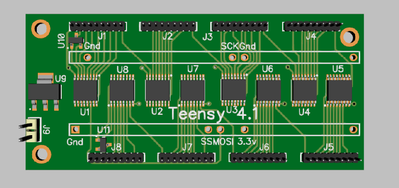 62 pin output 8 shift register timing board, work in progress. Regards, Marathonman |
|
|
|
Post by Marathonman on Nov 21, 2020 22:27:16 GMT -6
Holy crap i am tired, have been fitting and welding pipe all day. just thought i would Give update on 8 shift reg board. below is nearly finished board. this thing is small, like barely bigger then a Teensy 4.1.  Still work in progress. Regards, Marathonman |
|
|
|
Post by Marathonman on Nov 22, 2020 15:53:29 GMT -6
Finally taking a day off, am so tired and sore. Finished the board design, trying to make the board compact makes for some ruff routing. the final board below at a L-71.12 mm x H-31.59 mm with the Teensy occupying most of the footprint. the Teensy dimensions are L-61.66 x H-17.78 so you see the board is not much bigger allowing only for the 9 pin connectors and the voltage regulator. if you feel the need to use this 62 pin shift register along with the code i previously posted which will compliment this design then by all means download the Gerber and shift code. remember to change the amount of pins and speed in the code to your liking. board design is with Diptrace free 4.0.0.5 latest. so if you want to change things just download and change. link to Gerber and Diptrace board file. ***** link***** this board will obviously connect to your transistor board that has a separate power supply. i am not finished with the high side driver design as test circuits are still in process for qualifying such boards. when i am satisfied with the design i will post final transistor boards and Gerber files also. Also according to PJRC you have to cut the line between the usb power and the rest of the board when supplying external power to the board which also includes the power in the usb line it self if the external power is supplied. you can also put a switch on the external power supply then shut off when using usb connections.   Regards, Marathonman |
|
|
|
Post by Marathonman on Nov 23, 2020 0:25:24 GMT -6
I must warn you that the circuit must follow the diagram i posted to the letter in order for it to function properly. either that or change the bit order and shift left to right. Diagram below is the order to build the circuit that matches the code and it will shift in the direction of the arrow when first switched on. if you do not follow the schematic the switching groups of 8 will be erratic.  The circuit is built or added to the right but the shifting is to the left to start (MSB). Regards, Marathonman |
|
|
|
Post by Marathonman on Nov 23, 2020 14:15:09 GMT -6
This is how the Teensy 8 shift register is going to look when the Teensy 4.1 is mounted to the board. of course the rest of the pins not used by the timing board will be sticking upward for your use on other things. the gap between the Teensy and the board will be the thickness of your standoff pins that connect it to the base board which is plenty of room for digital shift registers.  Regards, Marathonman |
|
|
|
Post by Marathonman on Nov 23, 2020 22:46:24 GMT -6
I have hit a snag as i was thinking it would be easy to find 1.27 mm female housing. well i was completely wrong. have searched for two days trying to find a small connector with no avail. seems i am going to have to change the pin spacing to 1.25 mm or even 1mm as those two pin housings are available. i personally think the electronics industry is completely pathetic in this area selling 1.27 mm pins and no mating housing for them.
i have found both 1.25 and 1 mm on Aliexpress that are small enough housing to fit in the space provided. it can be changes by replacing part in DipTrace or if anyone needs it done i can do it for you just give a shout out.
remember these are all low voltage, low amperage digital lines going to either logic level transistors or logic level high side driver so the small size is not problem.
Regards,
Marathonman
|
|
|
|
Post by Marathonman on Nov 25, 2020 23:13:56 GMT -6
Please remember folks when designing your circuits and boards that the ends have to be on for a longer period to mimic the rotation of the mechanical version as the ends have an on time of three to four times longer then the contacts in the middle. this is why on the 8 shift register board i designed and posted has two end channels connected through a double diode to a single output (both ends). along with shifting two bits at a time for overlap, they are shifted to the end channels by two bits at a time so what this does is have the single end channel on for three times longer then the middle channels.
this action will cause the magnetic field being swept back and forth to have a sort of pause of delay in the sweep which causes an inductive roll off in the secondary giving it a nice sine wave shape that mimic your standard AC of today. if you do not do this your output will not be sine wave shaped like it should be, the whole reason to do this is to replicate the exact function and actions of the mechanical brush rotation as Figuera intended.
Below video is the video previously posted but slowed down to show the timing overlap to avoid sparking and or current disruption incorporating double diodes on the ends in the board design to mimic the brush rotation.
if you are to do it right, then do just that, do it right.
Regards,
Marathonman
|
|
|
|
Post by Marathonman on Nov 28, 2020 21:02:43 GMT -6
In the middle of all this cutting trace external power crap on the Teensy 4 and 4.1 i decided to add a dip switch on my board for that very purpose. if i need to update the program all i need to do is kill the external power and flick the switch on the Teensy which reconnects the USB power to the Teensy built in voltage regulator. i think this is the most sane solution to this problem i can think of by adding a dip switch, solder pads which will get connected to the underside of the Teensy USB square pads. even if it is not i still think it is a good idea for me and my project.  Regards, Marathonman |
|
|
|
Post by Marathonman on Nov 30, 2020 18:19:38 GMT -6
So as you people can see by now not only is the Coding extremely handy being able to use with "ANY" Arduino, it can also be modified to your speed, liking and tap count of your part G. since i have a custom C core that has a wide flat surface and large diameter loops, i can have less windings on part G with greater inductance per loop. this cuts down on my demand for more loops then if i had a smaller core. also as you can see the program/ board runs fine even with very long connecting wire like in the video which will be even better when put on a permanent board with very short traces. by having the transistor boards right below the timing board you can employ short runs of ribbon cable at 1.25 mm and connectors which can be ordered here.... link ........ at any size/pin count you need 1.25mm Pitch Connector Micro JST Horizontal Straight Pin or right angle just search. EDIT: link fixed. Regards, Marathonman |
|
|
|
Post by Marathonman on Dec 1, 2020 21:21:47 GMT -6
I am so F-in sick and tired from being blocked on certain sites. all power elites can kiss my big white ass as i am being blocked from Aliexpress now. seems i have to order from another computer as they keep trying to bomb mine or do a lot of blocking.
Pissy small men run our countries that do not have the balls to look a real man in the face hiding behind walls like a panty wearing bitch that they are..
Marathonman
|
|
|
|
Post by Marathonman on Dec 2, 2020 17:20:13 GMT -6
Seems like someone heard me as not only a hour later after i posted i suddenly was able to get on Aliexpress and log in. of course after i deleted ethernet drivers and reinstalled, did BS scan and removed something that was not suppose to be there thanks to Avast boot time scan.
found a really good shift register chip from of all people Toshiba part # TC74VHC595F(EL,K,F. it is 2 to 5.5 volt capable and can hit a blazing 185 mhz that sells for .65 cents in an SOP 16 and SSOP 16 package.
Nexperia has one 74VHC595 that has Schmitt-Trigger inputs with 2- 6 volts. it also has DHVQFN16 which is smaller then a knat's ass that i can not solder as that is way to small for my eyes.
Personally i like the Fact that Toshiba stepped up to the plate and offered one with so much headroom and i my type of package for my board.
Regards,
Marathonman
|
|
|
|
Post by Marathonman on Dec 4, 2020 0:27:52 GMT -6
Major update;
In the code i posted last week or so on the SPI shifting code and video, i forgot to tell people that one more line has to be changed in order to use 8 shift registers. in the code i have (SPI.transfer(&temp, 6); //Send the buffer to the registers)
this has to be changed to (SPI.transfer(&temp, 8); //Send the buffer to the registers) to reflect the number of shift registers used. i have 6 so it was great for me but when i added the other two shift registers the code shifting was all Willy Wonka. easily fixed.
I am so sorry for not catching this earlier people so all who downloaded it that plan on using 7 or 8 shift registers please change this line to reflect your register count.
also the video i posted on Youtube was updated to show 8 shift registers BO's for a total of 64 bits being shifted back and forth.
PLEASE SEE NEW VIDEO @ 64 BIT SHIFT.
Regards,
Marathonman
|
|
|
|
Post by Marathonman on Dec 5, 2020 18:28:28 GMT -6
I think the 8 shift register board and the code is a good combination and starting point for someone looking to get into the electronic switching of part G without all the fuss of creating their own from scratch. with the code and board anyone can choose what ever amount of taps or outputs you need from 2 to 64 not counting the end overlap. all you have to do is change the code to your desired pin count and your off and running with your first active inductor controller.
the next move in this evolution is the addition is to mimic a second brush from the secondary feed back into part G which is a good point to consider. when designing your transistor boards please remember that the voltage in the system will climb higher then that of the starting potential because of the forward biasing to the high side. build your transistor circuits to accommodate this potential rise
Regards,
Marathonman
|
|


